New optoelectronic devices for the Near and Mid-Infrared spectral range open completely new possibilities for portable sensors creation. Using infrared LED-PD optopairs allows developing an instrument that is smaller, less expensive and energy-saving.

Technology
LED Microsensor NT possesses the full cycle of technological processes needed for creation of LEDs and PDs from the very beginning to complete products.
The main technological stages.
1) The first and the key technological stage of diodes production is the growth of epitaxial layers. Diode heterostructure is formed by sequential epitaxy of semiconductor layers on the surface of a crystal substrate. We use liquid phase epitaxy (LPE) and metallorganic chemical vapor deposition (MOCVD) for epitaxial growth.
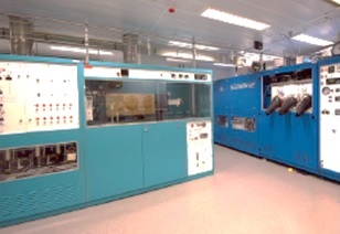
Epitaxial growth setups used by LED Microsensor NT
Using GaInAsSb/AlGaAsSb-based heterostructures lattice-matched to GaSb substrate allows us to create LEDs for 1600-2400 nm spectral range while InAsSb/InAsSbP-based lattice matched to InAs substrate allows us to create LEDs for 2800-5000 nm spectral range. There is a gap from about 2400 to 2800 nm due to existence of immiscibility region for GaInAsSb-based solid solutions which depends on the epitaxy temperature and compound composition.
2) The second technological stage is post-growth processing. It includes deposition of contact systems, photolithography to form grid, selective etching and splitting wafer into chips.
2) The second technological stage is post-growth processing. It includes deposition of contact systems, photolithography to form grid, selective etching and splitting wafer into chips.
Semiconductor wafer after the photolitography stage
(LED chips with ring top contacts)
3) The third technological stage is packaging. This stage includes mounting of chips on packages and bonding of contacts.
Mounting of chips on packages
4) The last and indispensable stage of the technological process cycle is quality control. Learn more >>